top of page

RIGID & FLEX PCBs
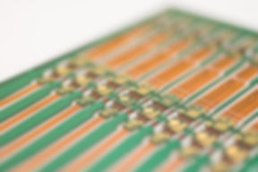
Twist it, bend it, and shape it — COFAN’s flexible PCBs are able to bend, but not break that’s necessary for a growing segment of electronics (like bendable TVs and phones). It isn’t all about being flexible though, as products need to be flexible in one area, but rigid in the next. COFAN offers rigid-flex for when you need just the right amount of flexibility and rigidity.


Fabrication Capabilities
Item | Standard |
|---|---|
Layer to Layer Registration Tolerance | +/- 75 um (for multilayer mass production) |
Layer Count | Standard: 1 – 4 layers (Capabilities: 1 - 6 layers) |
Material | Polyimide (variety of brands available) |
Plating finishes | Copper, Gold, Nickel, Silver, Tin, Tin-lead |
Minimum Drilled Hole | 100um(Finished) |
X-Y inspection tolerance | ± 75 um |
Minimum Line Width/ Spacing | Standard: 100 um Capabilities: 40.6 um (1/3-1/2 OZ conductor) |
Drilling/punching tolerance | ± 50~75 um |
Shielding | RFI / EMI provides 70(+) DB isolation from 50MHz to 12 GHz |
Controlled impedance | 40 ohms to 100 ohms |
Aspect Ratio | 9:1 |
Max Panel Sizes | Single Sided: 500 mmX 2000 mm Roll to roll is available for single sided Double or Multilayer: 480mmX 480mm |
FPC Design Guidelines
Button Plate Trace/Space and Thickness
Design Rule Parameter | Drawing/Pictures | Production Zero Base (µm) | Leading Edge (µm) |
|---|---|---|---|
Min. Space width between Traces ( >= 12um Cu Foil) | FPC DR 1_Trace Width & Space | 50 | 40 |
Min. Space width between Traces ( >=9um Cu Foil) | FPC DR 1_Trace Width & Space | 30 | 25 |
Min. Space width between Traces ( <= 18um Cu Foil) | FPC DR 1_Trace Width & Space | 60 | 50 |
Max. Plated button finished thickness (above base copper) | FPC DR_Button Ht | 20 | 20 |
Min. Trace width ( >= 9um Cu Foil) | FPC DR 1_Trace Width & Space | 30 | 40 |
Min. Trace width ( >= 12um Cu Foil) | FPC DR 1_Trace Width & Space | 50 | 50 |
Plated Through Hole (PTH)
Design Rule Parameter | Drawing/Pictures | Production Zero Base (µm) | Leading Edge (µm) |
|---|---|---|---|
Min. Mechanical Drilled PTH Diameter | FPC DR_PTH | 150 | 100 |
Min. Laser Drilled Via Pad Size (Panel Plate) | FPC DR_PTH | 450 | 350 |
Min. Laser Drilled Via Pad Size (Button Plate) | FPC DR_PTH | 400 | 300 |
Min. Laser Drilled PTH Diameter | FPC DR_PTH | 75 | 75 |
Min. Mechanical Drilled Via Pad Size (Panel Plate) | FPC DR_PTH | 300 | 275 |
Min. Mechanical Drilled Via Pad Size (Button Plate) | 225 | 175 (LDI) |
Copper to Copper / Holes / Slot / Bds Outline Clearance
Design Rule Parameter | Drawing / Pictures | Production Zero Base (µm) | Leading Edge (µm) |
|---|---|---|---|
Min. Trace/Ground/Via Pad to SMD Component Pad Edge (Photoimaged Mask) | FPC DR_Cu/SMD Pad | 100 | |
Min. Copper Edge to outline Edge | FPC DR_ Cu to Bds Outline | 200 | 150 |
Min. layer to layer registration tolerance - 3 to 6 layers | FPC DR_ Lyr_lyr registration | 75 | |
Min. layer to layer registration tolerance - 2 layers | FPC DR_ Lyr_lyr registration | 50 | 30 |
Min. space from via pads/trace/grounds to ground (I/L <=18um Cu Foil) | FPC DR_ T-V_V-V_VTG-G | 75 | |
Min. space from via pads/trace/grounds to ground (O/L <=18um Cu Foil, button plated) | FPC DR_ T-V_V-V_VTG-G | 75 | |
Min. Copper edge to NPTH or Non-Plated Slot Edge | FPC DR_ Cu/Bds edge to NPTH or non-plated slot | 200 | 150 |
Min. Via Captured Pad to Via Captured Pad | FPC DR_ T-V_V-V_VTG-G | 100 | 75 |
Min. Non-plated slot or NPTH edge to outline edge | FPC DR_ Cu/Bds edge to NPTH or non-plated slot | 200 | 150 |
Min. trace to via captured pad ( I/L <= 18um Cu Foil) | FPC DR_ T-V_V-V_VTG-G | 100 | 75 |
Min. trace to via captured pad ( O/L <= 18um Cu Foil, button plated) | FPC DR_ T-V_V-V_VTG-G | 100 | |
Min. trace to via captured pad ( O/L finished thickness <18um / >= 40um) | FPC DR_ T-V_V-V_VTG-G | 100 | 75 |
Min. SMD Component Pad to SMD Component Pad (Coverlay) | 600 | 400 | |
Min. SMD Component Pad to SMD Component Pad (Photoimaged Mask) | FPC DR_NSMD Space | 200 | 150 |
Min. Trace/Ground/Via Pad To NSMD Component Pad Edge (Coverlay) | FPC DR_NSMD Space | 150 | |
Min. Trace/Ground/Via Pad To NSMD Component Pad Edge (Photoimaged Mask) | FPC DR_NSMD Space | 100 | |
Min. Trace/Ground/Via Pad to SMD Component Pad Edge (Coverlay) | FPC DR_Cu/SMD Pad | 200 |
Soldermask / Coverlay / Stiffener
Design Rule Parameter | Drawing / Pictures | Production Zero Base (µm) |
|---|---|---|
Min. Space Between Soldermask Edge to Component pad edge | FPC DR_ SM/CV & Tolerance | 50 |
Min. Stiffener edge extention beyond all supported Cu pad edge | FPC DR 82 | 500 |
Min. Stiffener to Stiffener Gap | FPC_DR80 | 1500 |
Min. EMI Shielding film edge to Component Pad edge | FPC DR 39_40 | 500 |
EMI shielding film placement tolerance | FPC DR 39_40 | ±300 |
Min. Stiffener Edge to Start of Bend | FPC_DR80 | 500 |
Min. Stiffener Edge to Airgap edge | FPC_DR80 | 1000 |
Min. Coverlay Width (Dam) | FPC DR_ SM/CV & Tolerance | 300 |
Min. Space Soldermask to NPTH or Non-Plated Slot | FPC DR_ SM/CV & Tolerance | 75 |
Min. Soldermask Width (Dam) | FPC DR_ SM/CV & Tolerance | 100 |
Coverlay to outerlayer pattern alignment Tolerance | FPC DR_ SM/CV & Tolerance | ±150 |
Min. Space Coverlay to NPTH or Non-Plated Slot | FPC DR_ SM/CV & Tolerance | 250 |
Soldermask to outerlayer pattern alignment Tolerance | FPC DR_ SM/CV & Tolerance | ±50 |
Max Coverlay opening size Tolerance (Including the adhesive flow) | FPC DR_ SM/CV & Tolerance | 130 |
Minimum coverlay opening size | FPC DR_ SM/CV & Tolerance | |
Stiffener placement tolerance | FPC_DR80 | ±300 |
Min. Space Between Coverlay Edge to Component pad edge | FPC DR_ SM/CV & Tolerance | 150 |
Minimum soldermask opening size | FPC DR_ SM/CV & Tolerance | 75 |
Tooling for Profile
Design Rule Parameter | Drawing / Pictures | Production Zero Base (µm) | Leading Edge (µm) |
|---|---|---|---|
Outline Tolerance | FPC DR_ FPC outline | ±100 | ±50 |
Max. Slot Length (# x Width)? | FPC DR_Slot Width/Length | 6 times | |
Min. Slot Width | FPC DR_Slot Width/Length | 500 | |
Hole / Slot Edge to Outline Tolerance | FPC DR_ FPC outline | ±80 | ±50 |
Min. Hole / Slot Edge to Outline Distance | FPC DR_ FPC outline | 500 | |
Hole / Slot to Hole / Slot tolerance | FPC DR_ FPC outline | 80 | |
Min. Hole / Slot edge to Hole / Slot edge distance | FPC DR_ FPC outline | 1000 | |
Punched Hole / Slot Position Tolerance | FPC DR_ FPC outline | 80 | |
Punched Hole Diameter tolerance | FPC DR_ FPC outline | ±50 | |
Min. Punched Hole Diameter | FPC DR_ FPC outline | 500 | |
Min. Inside Corner Radius | FPC DR_ FPC outline | 400 | |
Min. Outside Corner radius | FPC DR_ FPC outline | 200 |
Others
Design Rule Parameter | Drawing / Pictures | Production Zero Base (µm) | Leading Edge (µm) |
|---|---|---|---|
Min. total contact bond area (cm2) per cm2 of effective EMI Shielding Film surface | FPC DR 89_90 | 0.01/contact | |
Min. Cu Edge (exclude trace thru' airgap) to AirGap Edge -- > 4 layers | FPC DR_Cu/Air Gap Distance | 1500 | |
Min. Cu Edge (exclude trace thru' airgap) to AirGap Edge -- 2 to 4 layers | FPC DR_Cu/Air Gap Distance | 1000 | |
Min. Cu Edge (outside of Stiffener footprint) to Stiffener Edge | FPC DR 81 | 500 | |
Min. AirGap Length for 5 to 6 Layers FPC | FPC DR_Air Gap Length | 5000 | |
Min. AirGap Length for 3 to 4 Layers FPC | FPC DR_Air Gap Length | 3000 | |
Min. single contact bond area (mm2) with EMI Shielding Film | FPC DR 89_90 | 1 | |
Silkscreen alignment to board outline (tolerance) | ±500 | ||
Max. Trace Width in Static bend region only (finished thickness >18um / <= 40um) | FPC DR_Trace Width at Bend | 250 | |
Max. Trace Width in bend region (<= 12um ED or RA Cu Foil) | FPC DR_Trace Width at Bend | 100 | |
Min. Ground opening edge to Outline edge | FPC DR_Circular/sloted gnd | 200 | |
Max. Ground to ground pitch | FPC DR_Circular/sloted gnd | 700 | |
Min. Ground to ground pitch | FPC DR_Circular/sloted gnd | 625 | |
Max. Ground opening diameter | FPC DR_Circular/sloted gnd | 500 | |
Min. Ground opening diameter | FPC DR_Circular/sloted gnd | 200 | |
Max. space width of Parallel trace ground | FPC DR_Circular/sloted gnd | 200 | |
Min. space width of Parallel trace ground | FPC DR_Circular/sloted gnd | 125 | |
Max. width of Parallel trace ground | FPC DR_Circular/sloted gnd | 500 | |
Min. width of Parallel trace ground | FPC DR_Circular/sloted gnd | 200 |


bottom of page